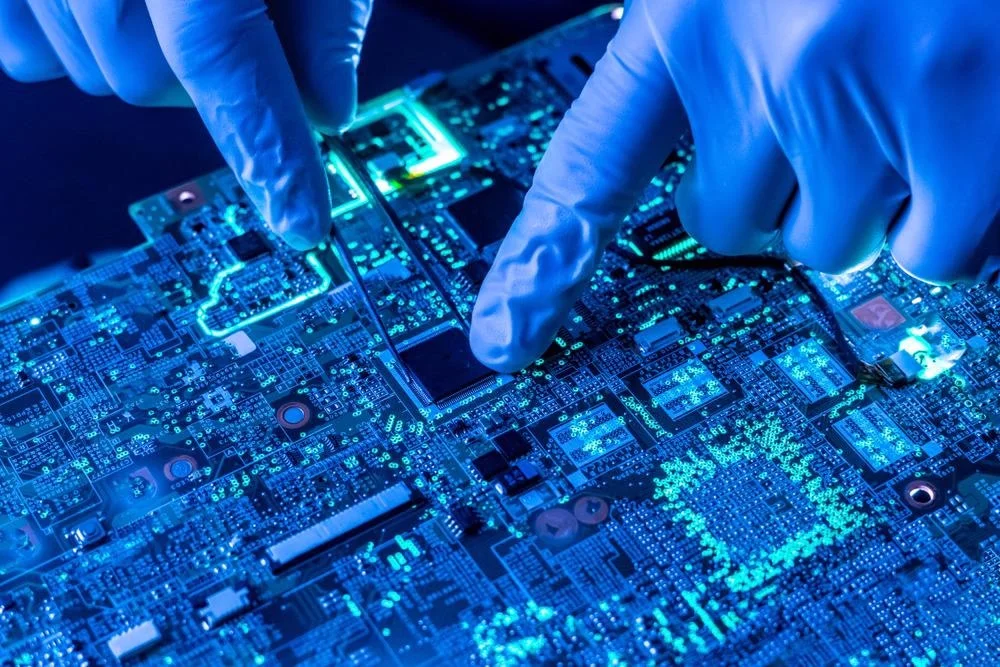
Building a chip fab (short for semiconductor fabrication plant) is a complex and highly specialised undertaking that involves a wide range of technologies, equipment, tools, and processes. Here are some of the key components required in building a chip fab:
Cleanroom: A chip fab requires a cleanroom, which is a controlled environment designed to minimise airborne particles and contaminants that could damage the delicate semiconductor wafers. The cleanroom must be equipped with air filters, air showers, and other specialised equipment to maintain a highly controlled and clean environment.
Lithography equipment: Lithography equipment is used to print the intricate patterns that make up the circuits on a semiconductor wafer. This includes photolithography equipment, which uses light to transfer a pattern onto a wafer, and more advanced techniques such as electron beam lithography and extreme ultraviolet (EUV) lithography.

Etching equipment: Etching equipment is used to remove layers of material from the surface of a wafer to create the desired pattern. This includes equipment such as plasma etchers and wet etchers.
Deposition equipment: Deposition equipment is used to deposit thin layers of material onto the surface of a wafer to create the desired circuitry. This includes techniques such as chemical vapour deposition (CVD), physical vapour deposition (PVD), and atomic layer deposition (ALD).
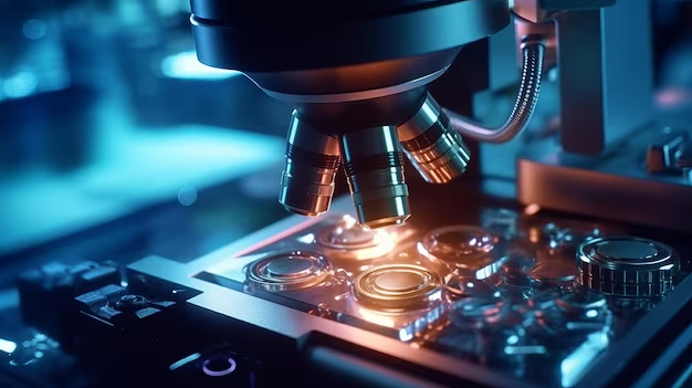
Metrology tools: Metrology tools are used to measure the thickness, shape, and other characteristics of the features on a wafer. This includes tools such as scanning electron microscopes (SEM), atomic force microscopes (AFM), and optical microscopes.

Packaging and testing equipment: After the semiconductor wafers are processed, they need to be packaged into chips and tested for functionality. This requires specialised equipment such as die bonding machines, wire bonding machines, and automated test equipment (ATE).
Water treatment and distribution systems: A chip fab requires a significant amount of water for its various processes, and the water must be highly purified and treated to ensure it is free of contaminants that could damage the wafers. This requires specialised water treatment and distribution systems.
Waste treatment systems: A chip fab generates a significant amount of waste, including chemicals and gases used in the various processes. These waste materials must be treated and disposed of in an environmentally responsible manner, which requires specialised waste treatment systems.
Building a chip fab requires a wide range of specialised technologies, equipment, tools, and processes, all designed to create a highly controlled and clean environment for processing semiconductor wafers. The cost of building a chip fab can run into billions of dollars, and requires significant expertise and resources to undertake successfully.


